Development Process
IoT solutions
Feasibility studies
The design of new products relies on the extensive use of accurate computer simulation models. Our engineering staff has a unique knowledge in electromagnetic simulation and numerical modeling gained through years of experience working on embedded antenna designs and general RF problems in both industry and academia. Every aspect of the electrical design is considered by our proprietary simulation models – from the geometry and material characteristics of the antenna enclosures to the effects of parasitic reactance on printed circuit board traces. We also consider the statistical variation of component tolerances in actual production.

Development of simplified 3-D simulation models
Investigation into design trade-offs
Antenna optimization based off customer provided bounds
Estimation of user proximity effects on antenna performance
Preliminary assessment of compliance with respect to performance requirements
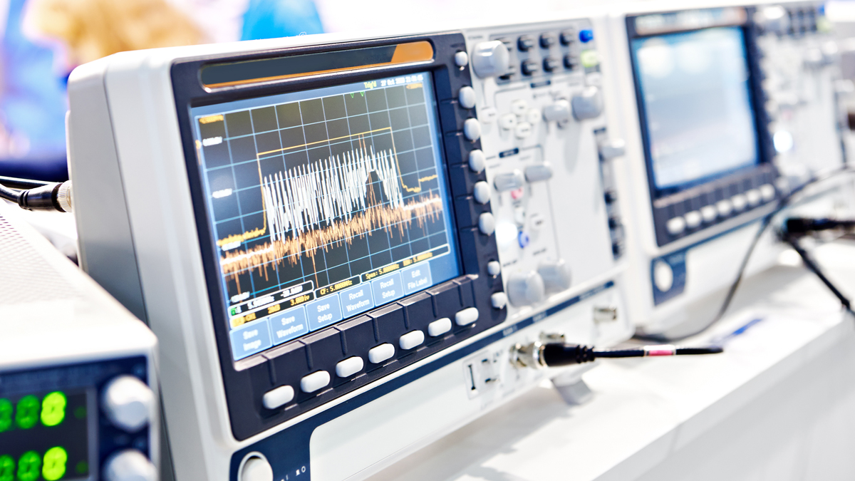
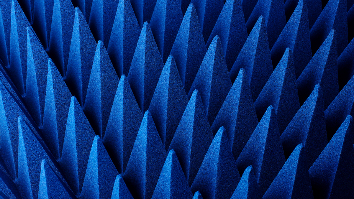
Chamber Testing
Maxtena has in-house the latest in antenna and RF measurement capabilities. We use the SATIMO Starlab Anechoic Chamber to measure radiative characteristics of the antenna for both passive and active systems. We are also equipped to provide you with TRP and TIS measurements.
Multiple antenna correlation and efficiency
3-D complex antenna pattern
Antenna input response
TRP/TIS measurements
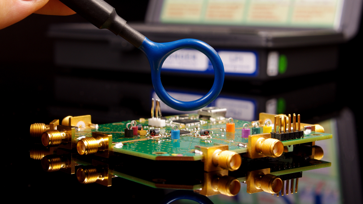
Prototyping
By leveraging the most advanced electromagnetic simulation software available, we can accurately predict the performance of new designs before any hardware is built. Prototyping is then used to verify the correlation between the design and final product. Our in-house measurement capabilities allow for quick turn prototype validation. In addition to antenna design, we provide antenna integration support for clients that require a high level of device integration.